It looks like you're using an Ad Blocker.
Please white-list or disable AboveTopSecret.com in your ad-blocking tool.
Thank you.
Some features of ATS will be disabled while you continue to use an ad-blocker.
0
share:
solar.anu.edu.au...
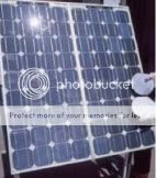
Sliver® cells address the major issue relating to the uptake of solar electric systems – the cost. Sliver® cells use up to 90% less silicon compared with mono crystalline cells of equivalent output resulting in lower module costs.
Sliver® cells were invented and developed by the Centre for Sustainable Energy Systems (CSES). Origin Energy, an Australian energy company, has committed $35 million to a manufacturing plant in Adelaide, and modules made of Sliver® cells will be commercially available from 2005.
The output of 72 conventional cells is the same as that from 2 wafers when the wafers are manufactured into Sliver® cells.
Flexible modules can be created by suitable encapsulation of the Sliver® cells (which are flexible due to their thinness).
Building-integrated Sliver® modules take advantage of the fact that any degree of module transparency can be easily achieved by adjusting the Sliver® cell spacing.
solar.anu.edu.au...
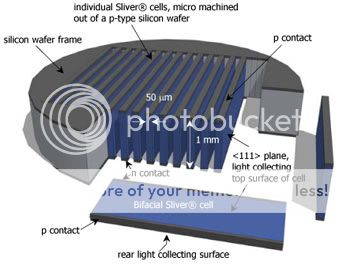
The invention of Sliver solar cell technology in 2000 by Dr Klaus Weber and Professor Andrew Blakers of the Australian National University is a fundamental breakthrough. Sliver cell technology uses standard materials and conventional techniques in novel ways to create thin single crystalline solar cells with superior performance at significantly reduced cost. Sliver cells are fabricated on single crystal silicon – the gold standard of the PV industry. Sliver modules are manufactured using techniques adapted from conventional module manufacture. Mature Sliver modules will use only conventional materials. Sliver modules can be efficient, low cost, bifacial, transparent, flexible, shadow-tolerant and light-weight. Sliver technology has the potential to be a comprehensive long-term solution for PV. Standard single crystal silicon wafers around 1 mm thick are used as the starting material for the Sliver cell process. Low cost micromachining methods are used to create many narrow parallel grooves that extend vertically through the wafer but do not extend to the wafer edge. The grooves lead to the creation of an array of thin, parallel, silicon strips, referred to as “Slivers”, confined in the wafer, and held in place at their ends by the un-grooved part of the wafer, referred to as the wafer frame. The entire wafer, containing up to several thousand Slivers, is then processed using standard techniques to turn each of the Slivers into a solar cell.
[. . .]
The key to understanding the significance of Sliver technology from the cell processing perspective is to recognise the fundamental difference between conventional cell processing and Sliver cell processing. In the conventional cell process, cells are formed on the wafer surface – essentially a 2-dimensional process. In the Sliver cell process, cells are formed in the wafer volume – essentially a 3-dimensional process, which produces a dramatic increase in the active surface area of solar cells per unit volume of silicon consumed and per wafer that is processed.
Strike one up for the Aussie's, I say.
I thought having a solar backpack would be cool, (I was looking for flexible solar panels and stumbled on this) but this technique has heaps of potential uses. Everything from building/architectural to compact, flexible solar chargers for phones, ipods etc.
solar.anu.edu.au...
[edit on 15-4-2006 by fingapointa]
NREL is working on the next generation solar cells: a 80-96% efficient Rectenna solar cell:
www.nrel.gov...
www.nrel.gov...
This is a must read for serious solar power supporters. With this solar cell a 3 panels would run the house, split water for the hydro-car and you could even sell electricity back to the grid.
www.nrel.gov...
www.nrel.gov...
This is a must read for serious solar power supporters. With this solar cell a 3 panels would run the house, split water for the hydro-car and you could even sell electricity back to the grid.
Thanks Bode, i'm very interested in solar power.
Reading the links now
Reading the links now
Bode, that stuff isn't next generation, they are at least 3 generations down the line. Right now the most efficent panel I've seen on the market to
date is around 14% efficient with it doubling every 7 to 8 years. Hopefully I'm wrong on the timeline and a big breakthrough happens, but I doubt it.
The similiarities in develop with the IT industry are there. Hopefully they can shorten the time for each doubling but I'm not that hopefull.
This tech is interesting. I'll have to research into it further. I don't have the time right now though, can someone please tell me how efficient these panels are.
[edit on 17-4-2006 by sardion2000]
This tech is interesting. I'll have to research into it further. I don't have the time right now though, can someone please tell me how efficient these panels are.
[edit on 17-4-2006 by sardion2000]
Actually Sardion,
I wouldn't put it past them to make a great leap forward on this next gen solar cell. Rectenna tech is diff from how solar cells work now and the tech that will make the new cells possible has just now become available. Read the PDFs if you get a chance.
[edit on 4/18/2006 by bodebliss]
I wouldn't put it past them to make a great leap forward on this next gen solar cell. Rectenna tech is diff from how solar cells work now and the tech that will make the new cells possible has just now become available. Read the PDFs if you get a chance.
[edit on 4/18/2006 by bodebliss]
I think that solar power is undoubtedly the single most important fuel of the future. We tried it for a while, but it fizzled out, and I believe it's
because we didn't research it out as well as we could have. I'm still an advocate for using solar power to generate hydrogen fuel from ocean water,
but that's another story.
There are a couple of noted houses in my state that are covered in so many solar panels that they actually generate enough electrical energy to donate it back into the matrix.
There are a couple of noted houses in my state that are covered in so many solar panels that they actually generate enough electrical energy to donate it back into the matrix.
new topics
-
Just spotted an unusual aircraft Melbourne Australia
Aliens and UFOs: 1 hours ago -
The truth lets admit it
Aliens and UFOs: 6 hours ago -
Mass Shooting Towson, Maryland - 7 shot, 1 possibly dead
Social Issues and Civil Unrest: 9 hours ago
top topics
-
Trump formally clinches Electoral College victory
2024 Elections: 14 hours ago, 17 flags -
Mass Shooting Towson, Maryland - 7 shot, 1 possibly dead
Social Issues and Civil Unrest: 9 hours ago, 5 flags -
The truth lets admit it
Aliens and UFOs: 6 hours ago, 3 flags -
Just spotted an unusual aircraft Melbourne Australia
Aliens and UFOs: 1 hours ago, 1 flags
0


